 Business
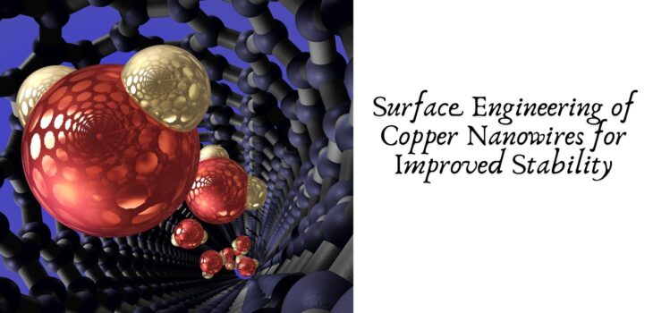
Surface Engineering of Copper Nanowires for Improved Stability
Introduction
Copper nanowires (CuNWs) are emerging as vital components in next-generation flexible electronics, transparent conductors, and energy devices due to their exceptional electrical conductivity, mechanical flexibility, and cost-effectiveness. However, their practical application is often hindered by poor chemical and thermal stability, especially under ambient conditions. Surface oxidation and degradation over time significantly reduce their performance, posing a major challenge for commercialization. This is where surface engineering plays a pivotal role. By modifying the surface properties of CuNWs, researchers can enhance their stability, improve durability, and unlock their full potential in demanding environments.
The Need for Surface Engineering in Copper Nanowires
Although copper is a superior conductor, it is highly susceptible to oxidation. When CuNWs are exposed to air, they form copper oxide (CuO or Cu₂O) layers, which impede electron transport and compromise device performance. In applications like touchscreens, solar cells, and sensors, long-term reliability is essential. Surface engineering addresses these issues by:
- Inhibiting oxidation through passivation layers.
- Enhancing compatibility with other materials for better integration.
- Improving mechanical robustness under bending or thermal cycling.
- Preserving electrical conductivity in challenging environments.
Without surface modification, the commercial viability of CuNWs remains limited.
Surface Engineering Techniques for CuNWs
Polymer Coating
One of the most accessible strategies involves coating copper nanowires with insulating or conductive polymers like polyvinylpyrrolidone (PVP), polyethylene oxide (PEO), or polyaniline (PANI). These coatings act as physical barriers against moisture and oxygen.
- Advantages: Easy to apply, flexible, scalable.
- Limitations: May slightly reduce electrical conductivity depending on the polymer used.
Metallic Shell Coating
CuNWs can be coated with a thin shell of a more stable metal such as silver (Ag), nickel (Ni), or gold (Au) using methods like electroless plating or galvanic replacement.
- Silver-Coated CuNWs: Offer superior conductivity and excellent oxidation resistance.
- Nickel-Coated CuNWs: Provide both thermal and chemical stability at a lower cost than silver.
- Challenges: Precise control of shell thickness is required to retain flexibility and minimize cost.
Atomic Layer Deposition (ALD)
ALD is a sophisticated technique that deposits ultra-thin, conformal films on nanostructures. Oxides like Al₂O₃, TiO₂, or ZnO are commonly used.
- Advantages: Excellent uniformity, precise control of film thickness, superior protection.
- Disadvantages: High cost and slow deposition rates limit industrial scalability.
Graphene or Carbon-Based Coating
Carbonaceous materials such as graphene oxide or reduced graphene oxide provide a conductive, flexible, and chemically resistant coating for CuNWs.
- Benefits: Enhance both mechanical and chemical stability, and maintain transparency.
- Research Focus: Developing efficient deposition techniques for uniform coverage.
Self-Assembled Monolayers (SAMs)
SAMs consist of organic molecules that bind to the copper surface and create a dense, hydrophobic layer to prevent oxidation.
- Common molecules: Alkanethiols and phosphonic acids.
- Pros: Minimal impact on conductivity; good moisture resistance.
- Cons: Typically offer only short- to medium-term protection.
Recent Advances and Breakthroughs
Recent research has showcased innovative hybrid techniques to enhance surface stability:
- Hybrid Coatings: Combining polymers with inorganic nanolayers (e.g., PVP + Al₂O₃) to create multilayer protection.
- Green Surface Treatments: Use of environmentally friendly, water-based passivation processes.
- Laser-Induced Nanowelding: Helps to fuse nanowire junctions and remove surface oxides, improving both stability and conductivity.
Application Impact of Surface-Engineered CuNWs
Surface engineering significantly improves the usability of CuNWs across multiple domains:
- Flexible Electronics: Maintains conductivity during repeated bending cycles.
- Touch Panels & Displays: Prevents degradation of optical clarity and conductivity.
- Photovoltaics: Enhances lifetime and efficiency of transparent electrodes in solar cells.
- EMI Shielding: Protects high-frequency devices from external interference while remaining chemically stable.
Challenges and Future Directions
Despite promising results, several challenges remain:
- Cost-Effectiveness: Some surface engineering methods, like ALD or noble metal coating, are expensive and time-consuming.
- Scalability: Uniform and large-scale coating of nanowires for commercial production is still under development.
- Eco-Compatibility: There is a growing demand for sustainable, non-toxic coating materials and processes.
Future research is focusing on:
- Multifunctional coatings that combine electrical, thermal, and chemical protection.
- Smart surface treatments that respond to environmental triggers (e.g., pH, humidity).
- Low-cost, roll-to-roll compatible methods suitable for industrial scale-up.
Conclusion
Copper nanowires hold immense potential as a cornerstone of modern electronics, but their long-term functionality hinges on effective surface engineering. By applying advanced coatings, protective shells, and functionalized layers, researchers can significantly enhance their chemical and physical stability. These advancements are not only essential for improving device performance but are also paving the way for widespread adoption of CuNWs in flexible displays, energy devices, and wearable technologies. As surface engineering techniques become more refined and scalable, copper nanowires are poised to transition from lab innovation to industrial mainstay.